
 Image 1 of 5
 Image 2 of 5
 Image 3 of 5
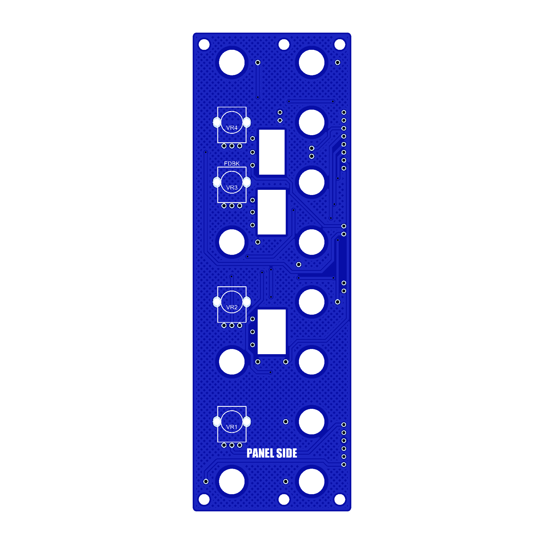 Image 4 of 5
 Image 5 of 5
Overview
This module is a modern adaptation of the classic 1973 Serge Triple Wave Shaper (TWS), originally developed by Serge Tcherepnin. As described in the 1982 Serge catalog:
“The Triple Wave Shaper (TWS) is a non-linear modifier that can transform a sawtooth wave into a sine wave. It comprises three independent wave-shaping circuits designed to process synthesizer waveforms or signals from preamplified instruments. Although initially intended to shape the output of early Serge oscillators, the TWS has proven to be a highly effective tool for modifying both electronic and acoustic signals. It is especially recommended for subtle timbral transformations that go beyond conventional oscillator/filter configurations.”
While originally conceived as a wave shaper, its applications extend much further. When multiple stages are connected in series, each additional stage introduces a further wave fold, offering extensive potential for harmonic enhancement and tonal complexity.
Single Stage: Basic waveform shaping.
Three Stages in Series: Increased harmonic content through successive folding.
Circuit Functionality
The module consists of three identical wave-shaping sections. When used individually, each section acts as an independent wave shaper. When connected in series, they function as a cascading wave folder.
Waveform Coupling Example:
The schematic illustrates all three identical sections of the Triple Wave Shaper, along with an example of how they may be interconnected.
Notable Historical Variations:
1973 Version:
Input pull-down resistors were 22k (compared to 100k in later versions).
AC-coupled outputs were mounted on the back of the jacks.
By 1975, AC coupling was discontinued and both output jacks were directly linked.
25k potentiometers were used for input level control.
Later Designs:
In two-column panel configurations, the second output was removed.
A “Join” switch was introduced to chain all three wave shapers internally.
Input potentiometers were moved to the front panel, although the PCB layout remained mostly unchanged.
LGE085 Version:
Incorporates additional 220k input resistors to support a Join switch without losing individual input functionality.
The Join switches connect the stages in series while preserving access to each stage’s input/output.
When using the Join switch, the second and third stage input pots are bypassed for the internally chained signal, but still allow additional signals to be mixed in.
Modernized input potentiometers (100k) bring input impedance in line with contemporary standards.
Added Feedback switch w/ Amount control routes signal back from the output to either the inputs of the second or third stages. Center position is off.
Construction
Pre-Assembly Checks:
Inspect the PCB for etching faults (e.g., shorts between tracks or incomplete traces).
Smooth any rough edges or splinters along the board perimeter.
Assembly Order:
Begin with the lowest profile components (resistors, diodes), followed by taller components. Pay close attention to the orientation of polarized parts, such as:
Electrolytic capacitors
Diodes
Integrated circuits
Transistors
Example Wiring
Wiring diagrams may include an optional off-panel Join switch. In the standard Join configuration:
Input: Bottom section
Output: Top section
Setup and Calibration
Join Switch Configuration: Ensure the each of the Join switches are turned off before calibration.
Signal Input: Feed a sawtooth waveform (audio frequency) into the IN jack of the top section.
Monitoring: Use an oscilloscope (preferred) or a multimeter set to AC voltage mode.
Adjustment:
Set the input level control fully clockwise.
Adjust the trim potentiometer until the output level approximately matches the input.
Repeat this process for each wave-shaping stage.
Control Voltage Inputs:
Control voltages applied to VC1 and VC2 will modulate the shape of the output waveform.
Assembled Modules are built to order, please be patient when ordering. Use the contact page if you have any questions or requirements!
** 4U Modular is a term used for the format most commonly known as “Serge Format” or “Loudest Warning Format”. Out of respect for the ever growing format, 4U Modular is the easiest way to refer to it. More Specifically it refers to the panel height and mounting hole style. 4U Modular will patch up just fine with other 4U "Serge" formats such as "Random Source", but it will not mount in RS boats or Buchla Boats (or power off Buchla power for that matter). An info page about this will be added to the website soon to make this a lot more easy to understand.
LGE085 Triple Wave Shaper DIY Information:
LGE085 Bill of Materials (Main & I/O Boards Combined)
LGE085 Main PCB Schematic
LGE085 Main PCB Layout w/ Designators
LGE085 Main PCB Layout w/ Values
LGE085C I/O PCB V2 Schematic (wiring diagram)
LGE085C I/O PCB Layout V2 w/ Designators
LGE085 Panel Art
Mechanical Parts BOM generally required for building Low-Gain Electronics Modules
Thank you to Guy D. , Ken Stone, Badger, Dean Batute and others for originally documenting & preserving Serge Modular Music Systems legacy!
Details:
PCB Size: 6” x 2”
Current Draw: TBD